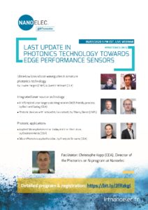
 Beyond high-performance computing (HPC) & data centers, Photonics technology is now ready to addresses also application in Consumer Electronics, Industrial, Automotive & Transportation, Smart city, Cybersecurity, Food & Beverage, and Medical Care. Optical sensors are well known for accuracy, sensitivity, selectivity, versatility, and speed of acquisition. Thanks to the development of integrated photonics, next generation of optical sensors will also improve compactness, lightweight, and low consumption.
During this webinar, after a glimpse of future prospects, Nanoelec speakers shared their latest results & performance obtained in integrated photonics technology: 300mm R&D and industrial fab, ultra-low loss waveguide, multi wavelength layer engineering with several waveguide materials (Si, Si3N4, SiGe, …), III-V material engineering and laser source integration, advanced electronic design automation tools and wafer-level testing.
> Foreword, by Christophe Kopp
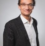
Christophe Kopp is director of the Nanoelec program dedicated to Integrated Photonics on silicium. Since 2001, he has been with the CEA-Leti, Grenoble, France, where he has been engaged to develop micro-optoelectronic devices for high-speed optical fiber communications. His researches have then been focused on integrated optics technology with the development of the CEA-Leti silicon photonics platform. In this field, he is author or co-author of more than 100 papers in scientific journals and international conference proceedings, two scientific books, and more than 30 patents. Since 2018, he is at the head of the section of new photonic applications with 80 research engineers/technicians and 20 PhD students in 3 laboratories to address lighting, display, sensing, communication and computing applications.
> Ultra-low loss silicon waveguides in a mature photonics platform, by Erwine Pargon (CNRS) & Quentin Wilmart (CEA)
Silicon photonics is a prominent technology for applications as diverse as Datacom, Lidar, or quantum computing. The transmission losses in sub-micrometer silicon waveguides is essentially due to scattering losses induced by waveguide sidewalls roughness. They are a limiting factor to achieve the low power-loss budget required for all the cited applications. Here we demonstrate that the introduction of high temperature H2 annealing treatment in the Si waveguide fabrication process allows to decrease the Si sidewalls roughness at the atomic scale, and consequently to reduce the waveguide propagation losses down to unprecedented low values of 0.1 dB/cm and 0.7dB/cm in rib and strip geometries. In addition, we demonstrate that the H2 annealing step can be introduced in the fabrication process of a 200mm photonic platform without compromising the performances of all the other main passive and active building blocks of the platform. This technological breakthrough opens the way to the manufacturing of high-speed, low-power optical interconnects for next generation communication systems and data interconnect but also to the fabrication of entangled photon pairs sources for quantum applications. Read the ppt from Erwine & Quentin
Erwine Pargon is an associate researcher at the “Laboratoire des Technologies de la Microélectronique” (LTM), a joint academic unit of the CNRS and Grenoble Alpes University in Grenoble, located in the CEA-Leti site in Grenoble, France. From 2019, she led the LTM etch group. Her research focuses on the development and characterization of plasma etching processes involved in the elaboration of advanced devices for microelectronic, photonics and photovoltaics applications. In particular, she worked on an important issue in plasma patterning, the pattern sidewalls roughness by proposing plasma strategies to minimize it or innovative metrology to measure it.
Quentin Wilmart received the Ph.D. degree in physics from Ecole Normale Supérieure, Paris, France in 2015. He joined CEA-Leti in 2016, working on design, fabrication and characterization of photonic integrated circuits. His current research interests include the use of silicon nitride and IIIV materials for high-speed optical communication and quantum photonics. He is an author or co-author of 23 journal and conference papers and holds several patents.
> Integrated laser source technology
III-V/Si Hybrid laser large scale integration in CMOS friendly process, by Bertrand Szelag (CEA)
In this contribution, we present the hybrid III-V/Si photonic platform developed in CEA-Leti. The overall integration is done in a fully CMOS compatible 200mm technology, scalable to 300 mm wafers, leveraging the large scale integration capabilities of silicon photonics. III-V material is integrated on top of a mature silicon photonic front-end wafer through direct molecular bonding enabling the monolithic integration of light sources. A modular approach is used in order to minimize the impact on the already qualified silicon-based devices. Collective III-V die bonding is proposed in this platform. CMOS compatible metallizations are used to form ohmic contact on n-InP and P-InGaAs. A fully planarized 2-metal-level BEOL is used on top of the laser. Read the ppt from Bertrand.
Bertrand Szelag heads Silicon Photonics Laboratory at CEA-Leti since 2018. He has been project manager in photonics between 2013 and 2018, after an experience as project mnagager at STMicroelectronics where he has been in charge consecutively of wafer foundry outsourcing and desing kit integration. He has a PhD in semiconductors physics presented ad INP-Grenoble
Photonic devices with reduced In, Ga content, by Thierry Baron (CNRS)
III-V semiconductors present interesting properties and are already used in electronics, lightening and photonic devices. Integration of III-V devices onto a Si CMOS platform is already in production using III-V devices transfer. A prospective way consists in using selective hetero-epitaxy processes to grow the III-V materials directly on Si and at the right place. To reach this objective, some challenges still needed to be overcome.
In this contribution, we will briefly review the different technologies compatible with large-scale integration to integrate III-V semiconductors to realize specific functions such as light emission and detection. An important aspect of the presentation will be devoted to MOCVD hetero-epitaxy of As based III-V compounds on large scale wafers. Selective deposition will also be considered to put the materials only at the place where it is needed. The potentiality of these two approaches for devices realization such as light emitting devices and photodetectors will be discussed. Read the ppt from Thierry.

Dr. Thierry Baron, is director of research at CNRS-Grenoble. He received his Ph.D. at University Grenoble Alpes in 1996. His thesis focused on II-VI semiconductor for optoelectronic applications and his post-doc at the University of Wurzburg (Germany) was on the fabrication and characterization of II-VI LEDs. He joined the CNRS in 1998 to work on the elaboration of silicon nanocrystals on insulating substrates, the study of their physical properties and their integration in memory devices. Then he investigated the catalytic growth of Si, Ge and heterojunction nanowires and their integration to demonstrate specific functions in an industrial environment. His current research focuses hetero-epitaxy of III-V semiconductor on silicon to improve electronic and optoelectronic devices.
> Photonic applications
Applied Silicon photonics For Today And For The Future, by Eleonore Hardy (CEA)
With the advent of technological advancements such as AI, machine learning, and 5G communication, we see the rise of cloud computing. Consequently this rise is increasing the demand for optical transceivers. With major technological advancements, it is possible for silicon photonics to answer the growing demand for high bandwidth and high data rate capabilities and gaining increasing market share. In the meantime, silicon photonics is evolving in order to address emerging applications with new demands in term of complexity and efficiency as such as quantum communications and novel neuromorphic functions for AI systems. This talk will give an overview of the applications of silicon photonics for today and for the future. Read the ppt from Eleonore.
Eleonore Hardy joined CEA-Leti in 2018 as a business developer in silicon photonics. She holds a Master’s degree in Engineering and followed a MS in Management & Innovation. Eleonore has been working in the optics and photonics industry since 2005 and previously worked for Philips in the Netherlands and for Varioptic (a BU of Corning) in China. During her career, Eleonore has been successful in creating long-term value in lasers in France, China and India for Quantel (Lumibird), and spectrometers in Europe and Asia for Resolution Spectra Systems. Eleonore is dedicated to developing new business opportunities in silicon photonics, especially for communications, sensing, high-performance computing and quantum applications.
Silicon Photonics applied to Lidar, by François Simoens (CEA)
3D perception is essential for a broad range of applications, from autonomous navigation to industrial and environmental monitoring or even augmented reality. Lidars (Light Detection and Ranging) provide such remote 3D imaging with high accuracy in angle and distance. In order to meet large volume market, lidars have to be smaller and low cost. Silicon photonics enables the integration of the key lidar functional blocks to realize a fully integrated, single-chip sensor. Such technology allows unprecedented high volumes at low cost with no moving part. This talk will give an overview of the challenges and the evolutions of lidar systems, and will illustrate the suitability of silicon photonics to offer very concrete opportunities for lidars. Read the ppt from François.

Dr. Francois Simoens is Executive Strategic Program Manager “Chip-scale lidar” at CEA-Leti, since 2019. François Simoens carried out seven years of R&D in the accelerator field in Saclay, before joining Grenoble in 2003 with the position of program manager and expert in infrared and THz sensors. From 2015 to 2018, he has been the Marketing and Strategy Manager for the imaging technologies and systems developed at Leti.


