

Some major advances in the integration of optical and photonic components onto silicon have been made over the past several years. A number of demonstrators have been built and tested, from low-loss waveguides, couplers, and other passive components to fast optoelectronic components like photodetectors and modulators operating at 25 Gbps in industrial environments and at more than 50 Gbps in the R&D.
However, the integration of an optical source (a laser) onto photonic circuits is a critical phase in the fabrication of complete transponder circuits. There are four ways to integrate a laser onto silicon:
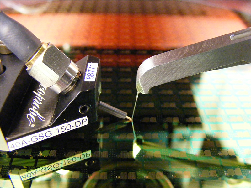
- Use a flip-chip bonding process to attach a complete laser to a photonic chip. Flip-chip processes are currently used in industrial manufacturing. However, each laser must be individually positioned on each optical circuit and must be very precisely aligned (to within 1 µm). Therefore, active alignment of the chip must be used, which reduces manufacturing throughputs to well below what CMOS processes would normally allow. Nevertheless, the method is suitable for relatively small circuit manufacturing volumes.
- Grow the III-V material required directly on the silicon circuit after circuit fabrication. With this approach, it is possible to fabricate the lasers directly coupled with the silicon waveguides using etching at the different scales. Lasers are obtained directly on the silicon wafers, eliminating the need for active alignment. However, defects resulting from differences in the atomic interface between the silicon and the III-V material create dislocations that substantially reduce laser performance. Research is currently underway to find a solution, with some encouraging results (quantum-dot lasers have been successfully fabricated, for example). This approach will require long-term R&D to be viable.
- Use germanium to fabricate the lasers. Germanium is a conventional material for silicon photonic circuits and results in efficient photodetectors (~1A/W at 1.3µm and 1.5µm). However, germanium is characterized by an indirect band gap. The material must be constrained in a specific way to make the band gap direct. Attempts to fabricate lasers on silicon using constrained germanium or a germanium-tin alloy are ongoing and some encouraging results have been obtained (laser emissions in suspended disks up to the tens of Kelvins). Several years of additional R&D will be needed to develop a germanium laser that operates at ambient temperature.
- Attach the III-V chips that already have the layers necessary for laser fabrication (quantum dots, stop layers, etc.) to the silicon photonic wafer. It is then possible to complete the laser fabrication processes on silicon at wafer level (compatible with batch manufacturing) with etching alignment tolerances (several nm). The initial chips are larger (mm²) than the lasers (µm²). This eliminates the need to position them precisely, making the approach suitable for high-throughput manufacturing.
IRT Nanoelec’s photonics program opted to focus on the fourth method in research that resulted in a high-power (> 4mW in the waveguide) very compact (< µm²) laser. The integration density is compatible with silicon photonic circuits, as is the production volume (wafer-level process). The research also demonstrated that the integration of the lasers enables the creation of CMOS-compatible electrical contacts. In other words, at the end of the fabrication line, several levels of metal interconnects that do not contain noble materials like gold and platinum and that are compatible with flip-chip processes can be created.