
Head of the new Photonic Application Sector at CEA-Leti and Director of the Nanoelec/Photonic Sensors program (c)UtopikPhoto/CEA
The “Photonic Sensors” program aims to expand the scope of the silicon photonics platform developed by Nanoelec since 2012 through the integration of innovative building blocks to address high volume optical sensor markets (Consumer Electronics, Industrial, Automotive & Transportation, Smart city, Cybersecurity, Food & Beverage, and Medical Care).
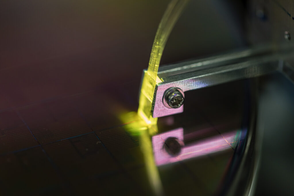
Key Technologies will address the development and demonstrations for integrated Lidars targeting consumer and automotive applications, inertial sensors and biochemical sensors for health and environmental applications.
In 2022, we demonstrated a 256-channel Optical Phased Array at 1,550nm consuming only 0.54W. We updated the Silphide and PIC 50G architecture design kits. We produced complete and functional LED structures at 700nm on 300mm wafer overcoming the N-doping obstacle, and demonstrated III-V epitaxy bonding on PIC with oxide gate in the 5-15nm range.
We also carried out the first functional integration of the DAN1 laser (III-V/SI hybrid components) on 200mm wafers.