

The Electronic Components and Technology Conference (ECTC) is the premier international event that brings together the best in packaging, components and microelectronic systems science, technology and education in an environment of cooperation and technical exchange. At ECTC 2023 (June 2023, USA), two studies conducted in the frame of Nanoelec were presented by CEA scientists:
-
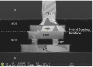
Hybrid bonding inteface after Cu-Cu bonding (c) CEA
Demonstration of a Wafer Level Face-To-Back (F2B) Fine Pitch Cu-Cu Hybrid Bonding with High Density TSV for 3D Integration Applications: The research team successfully fabricated a 2-Layers Face-To-Back (F2B) test vehicle (TV) by combining fine pitch Cu-Cu hybrid bonding technology with high density (HD) TSV. Three different stacked structures, built on 300 mm wafers, are needed to achieve the F2B TV. There are different Cu damascene levels that simulate back-end-of-line (BEOL) layers commonly used in 3D integration. Morphological characterizations have been carried out and highlighted the integrity of the 3D structure. F
urthermore, results of electrical tests on Kelvin and Daisy-Chain structures demonstrated a high connectivity. Kelvin and Daisy-Chain test structures are designed with either standard or fine pitch configuration (Pitch: 6 μm and 4 μm respectively) with hybrid bonding pad dimensions of 3 μm and 2 μm respectively. HD TSV dimensions are 1 μm in diameter and 10 μm in height.
-
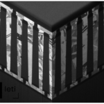
High Density TSV for 3D stacking architecture (c) CEA
Recent Progress in the Development of High-Density TSV for 3-Layers CMOS Image Sensors: Copper TSV in a via last approach were developed for advanced imaging applications. An aspect ratio of 10:1 was targeted with a diameter/space of 1μm/1μm (pitch 2μm) associated to a depth of 10μm. A test vehicle made of a single metal level on each side of a thinned Si substrate bonded onto a thick carrier was used to develop and optimize a process flow compatible with the constraints of a subsequent hybrid bonding process. An electrical resistance of 0.7 Ω (median value) was measured on Kelvin patterns and a yield of 100% was obtained on daisy chains made of 10 000 TSV. No failure was observed after 2000 h of HTS at 150 °C nor after 2000 cycles of TCT between -55 °C and +150 °C.
CEA-Leti, supported by Nanoelec, has developed an advanced hybrid bonding technology in collaboration with the IRT Nanoelec consortium. This innovation enables improved interconnection of integrated circuits and finds applications in various fields such as high-performance computing and photonics devices. Read more here.