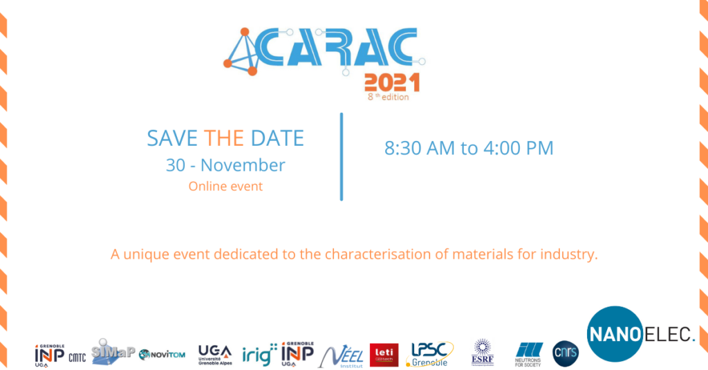
Dedicated to imaging techniques, the 8th edition of Carac has been held November 30, 2021. This year, the attendees had the opportunity to take part in a set of practice workshops focused on selected high performance techniques(tomography, chemical mapping, high-resolution topography and morphology…).
Carac Symposium, supported by Nanoelec/Characterisation program and its attached PAC-G platform, is the annual event dedicated to characterisation techniques that fit to electronics domain and beyond. Characterisation of new electronic components is essential to their design and ultimately to ensure their reliability. The increasing complexity of electronic components and technologies, as well as the diversification of materials and manufacturing processes in the More-than-Moore approach require characterisation that exceeds the performance of conventional laboratory equipment. To accurately correlate the micro and nanoscale characteristics of materials with the macroscopic properties of components, researchers need to gain in spatial resolution, detection capability and acquisition speed. This is why they use very specific beams of photons and neutrons from large instruments among the best in the world available on the scientific peninsula of Grenoble.

Agenda, Speakers & Abstracts
|
|
Speaker |
8:30 – 8:45AM | Welcome adress & Introduction |
Ennio Capria (ESRF), Conference Chair Hughes Metras, Director of Nanaolec |
Session 1 | 8:45– 10:00 AM | Each institute present its best case study
|
|
Session 2 | 10:00 -11:00 AM | Electron Microscopy for materials scienceAdvanced materials cover many fields of application. They meet specific high performance needs such as excellent mechanical, electrical, thermal or corrosion resistance for example. Materials are the basis of all industrial manufacturing sectors and step in at all levels of value chains. It is therefore strategic to position ourselves on the rapidly growing market for high added value materials, and with regard to the underlying scientific and technological knowledge, in the fields of energy, transport, environment, health, and information and communication technologies. This is why “advanced materials” are among the key technologies through which Europe intends to climb onto the world industrial podium. |
Stéphanie Kodjikian (Néel Institute/CNRS) |
11:00 – 11:15 AM break |
|
Session 3 | 11:15 – 12:15 AM |3D analysis of nanoscale materials using electron and FIB-SEM tomography techniquesThis tutorial will be divided in two parts: the first part will present the principles of electron tomography and FIB-SEM tomography, and their applications in materials science and biology. A review of state-of-the-art reconstruction algorithms and segmentation tools will also be presented. In the second part, a hands-on demo will be given using interactive Python notebooks and open-source packages. |
Zineb Saghi (CEA-Leti) |
Session 4 | 12:15 – 1:15 PM | Neutron Imaging and its applicationsNeutron imaging is a powerful non-destructive method for probing matter in 3D, capable of tackling questions from a plethora of scientific areas. A range of advanced imaging techniques are also rapidly developing and expanding the range of available contrast options, such as phase contrast, and polarised neutron imaging. Due to its non-destructive nature, it is possible to acquire multiple 3D volumes as the sample evolves, for example through chemo-thermo-hydro-mechanical loading, which in turn allows the spatio-temporally resolved quantification of processes. Recent technological developments even allow the simultaneous acquisition of highly complementary x-ray tomographies. This presentation will review the fundamental elements of neutron imaging, from the fundamental equations governing it, to the neutron production and detection. It will also attempt to provide an overview of the advanced techniques developed in recent years and provide an outlook of ongoing and future developments. |
Alessandro Tengattini (ILL/UGA) |
1:00 – 2:00 PM lunch break |
|
Session 5 | 2:00 PM – 3:00 PM | Scanning x-ray diffraction techniquesScanning x-ray diffraction techniques rely on fine spatial resolution to repeat the collection of scattering intensity or patterns obtained at several places in specimens under investigation. They have been boosted by the advance of brilliant synchrotron sources for two decades, the extreme high quality of X-ray optics elements and the ever growing fast and sensitive detector. Such spatially resolved single crystal diffraction techniques allow the determination of the structural parameters (crystal lattice parameters, strain or orientation) at the Nano- and micrometre scales. Two instruments operating at the European synchrotron (ESRF) will be presented. First, the kmap technique performed on ID01 beamline using a monochromatic beam provides a strain map from a huge and rapid rocking curve measurements on a chosen lattice planes family. Second, the Laue microdiffraction station on the French CRG-IF BM32 beamline uses a polychromatic beam to record the so-called Laue patterns – composed of a large number of lattice planes families 2D spots. These metrological techniques brings valuable insights on physical, chemical and mechanical properties of materials both with fundamental and technological aspects. Capabilities and applications of the techniques will be presented with last recent progress made in the data analysis. |
Jean-Sebastien Micha (IRIG/ESRF) |
Session 6 | 3:00 PM – 4:00 PM | X-ray probe and nano tomographySynchrotron radiation microtomography has emerged as the most powerful 3D characterization technique allowing very subtle structural changes in any type of material to be detected. The high flux and parallel beam produced by synchrotron facilities allows phase contrast imaging in multi-phase materials, and enables both ultra-fast image acquisition and high spatial resolution, at an energy that can be easily adjusted to the sample nature and experiment needs. |
Elodie Boller (ESRF) & Athanasios Papazoglou (Novitom) |


