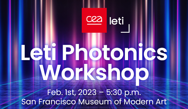
CEA provides a dedicated workshop as a side event at @Photonic West Conference. During his talk on Next Gen photonics platforms for rising applications, Bertrand Szelag, Integrated Photonics Program Manager @CEA-Leti, presents III-V material integration on Si photonics platform through direct bounding (wafer to wafer & die to wafer). Developed in the frame of Nanoelec, the process is available for 200 and 300 mm wafers. It is CMOS compatible ready for large scale integration.


