
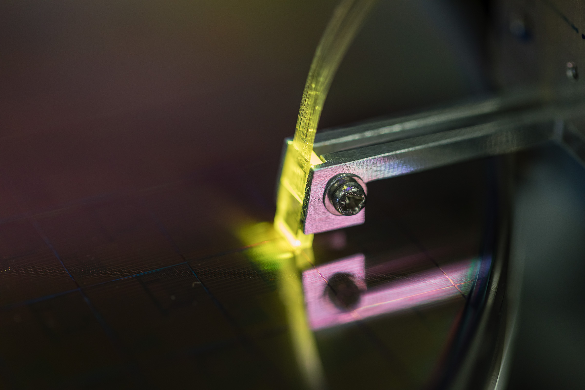

| New sensor opportunities based on large-scale 300mm silicon photonic technologies. Read more here | |
| Enrich our photonic prototyping and industrial platforms with key building blocks enabling new sensors to address Medtech, Environment, Consumers goods, Mobility (Lidars) and Computing | |
| • Miniaturize sensors • Diversify the fields of application • Manage the integration of thousands of functions on the same chip • Increase technology readiness level using CAD tools and enrich our device library including performance corners, fabrication process flow | |
| | Almae, CEA, CNRS, Siemens EDA, STMicroelectronics |
More on issues & context of the Nanoelec/Photonic Sensors program, here.