


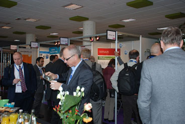
IRT Nanoelec once again attended the annual European 3D Summit held on January 23–25 on the MINATEC campus in Grenoble.
The plenary session, “Towards high-density interconnections,” offered up a review of the latest results of very-early-stage research on very-high-density integration for 3D design. Breakthrough technologies like hybrid wafer-to-wafer and chip-to-wafer bonding and bonding with self-alignment—developed under IRT Nanoelec projects—received generous attention.
High-density 3D integration is currently emerging as an industrial-scale solution for imaging and computing applications—but also for stacking memory circuits and for systems-on-chip.
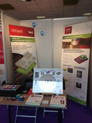
IRT Nanoelec also exhibited at a joint booth with Leti, providing an opportunity to showcase the research conducted under the 3D Integration program and, especially, the latest results obtained on our demonstrator systems. A fun presentation using Lego-like building blocks showed how, using new assembly technologies, circuits can be juxtaposed or stacked in virtually any configuration within the same enclosure.
Our 3D Integration program partners were also on hand at the event, exhibiting at their own booths and giving presentations (ST, SET, EVG).
 |
 |
Learn more at: http://www.semi.org/eu/european-3d-summit-2017