

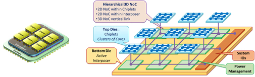
Mushrooming volumes of data have created a need for more complex circuits. One potential solution for server and Big Data applications is to combine different technologies and several chips to create more complex, efficient systems. The number of interconnections is growing, and chip surfaces are getting smaller and smaller. The use of an active silicon interposer makes it possible to integrate high-resolution redistribution layers, advanced components, and parts of circuits produced using proven technologies.
The IntAct demonstrator is made up of a manycore circuit partitioned using an active interposer.
The IntAct project is part of the IRT Nanoelec 3D integration program.
This type of 3D partitioning with an active interposer offers several benefits.
- Partitioning the circuit into smaller circuits that are tested and selected before assembly results in higher yields. The total system cost is also lower.
- The circuit is made using heterogeneous technologies: an aggressive technology for the 28 nm FDSOI processor cores, a mature 65 nm technology for the active interposer (which reduces costs while maintaining good yields and an intentionally-low fill rate), and aggressive 3D technology to ensure a good 3D interconnection rate.
- In addition, advanced functions can be added inside the active interposer. These include power management, rapid chip-to-chip interconnections, circuit infrastructure management (clock, reset, test, monitors), and rapid IO with components outside the circuit.
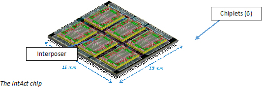
Here, the IntAct demonstrator circuit is a 3D circuit made up of six 28 nm FDSOI chiplets, each of which contains four clusters with four MIPS 32 bit cores. It also has a memory hierarchy with three coherent cache levels. The chips are 3D assembled on an active interposer made with a mature 65 nm technology and that integrates communication, power management (a new block), and testing and troubleshooting (stress, thermal performance, etc.). The communication functions (here, a 3D hierarchical network-on-chip) were developed for a previous 3D NOC demonstrator.
The IntAct circuit was made using a 3D technology with an aggressive 20 µm interconnection pitch, a face-to-face architecture for the microbeads, a 40 µm pitch for the through silicon vias with a 10:1 form factor, and backside routing.
The 20 µm pitch microbeads offer low-energy chiplet-to-chiplet communication with high data transmission speeds through the interposer. The interposer has 150,000 microbeads; 30,000 of them are dedicated to chiplet-to-chiplet interconnections and the rest are used for power management. Overall data transmission speeds of around 370 gigabytes/second are expected.
In terms of the connections to components outside the chip through the organic ball grid array substrate, 14,000 through silicon vias (electrical connections) are required.
The total estimated processing power is 100 GOPS (giga operations per second) at 20 watts in typical use scenarios.
A significant improvement in energy efficiency is also expected thanks to shorter communication distances with the 3D architecture and energy management that is closer to the computationnal load.
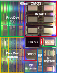
ITAC reticle containing the IntAct circuit and associated testing structures
In addition to the IntAct circuit (functional demonstrator), the reticle also contains test structures for the development of the technology, the electrical and RF characterization, and the assembly, reliability, thermal, and thermomechanical testing.
The initial results of the technological research have been published; additional results are forthcoming. Concerning the demonstrator, the functional and application test results are expected by end-2018. These results will position IRT Nanoelec as a leader in chiplet-based 3D integration.