Samples
PAC-G offers characterisation services spanning all pre-market (R&D) and manufacturing steps in the micro- and nano-electronics industry. This includes raw materials, processed materials, wafers, bare dies, stacks and finished components. Many of our characterisation techniques support in-situ studies for investigating manufacturing methods, product performance and failure. We can particularly add value when it’s necessary to understand certain phenomena.
Techniques
The four members of PAC-G offer a combined portfolio of more than 20 individual characterisation techniques that are available for use by industry. These fall into three categories: physical/chemical characterisation, imaging and irradiation.
Physical and chemical characterisation techniques can be applied to elemental analysis, thin film characterisation, crystal quality assessment, interface characterisation, stress/strain measurements and structural characterisation. For 2D and 3D imaging, PAC-G provides access to both X-ray and neutron imaging services, and at resolutions that are unavailable elsewhere in the world. This can be used for viewing working components, failure analysis and product qualification.
A key player in the high-reliability market, PAC-G provides irradiation services for the space and aeronautics industries, as well as for medical, automotive and mass storage applications. Irradiation services include neutrons (from 14 MeV to thermal neutrons), heavy / light ions and pulsed synchrotron focused x-ray beams. This makes them ideal for assessing the SEE sensitivity of chips and other electronic components, as well as for fault injection. Please click on the headings below to see the individual techniques that are available within each category.
X-ray Topography (XRDI, XRT)
Main Applications
- Statistical characterization of nano-objects, determination of the porosity
- Quantitative information on the average size, size distribution, kinetics of any defects or pattern inside a matrix
- Applications in yield enhancement, modeling and process optimisation
High resolution X-ray Topography
(HR-XRDI)
Main Applications
- Local and global information on strain and Stress
- Fast and continuous mapping of lattice strain and tilt
- Nanostructure, phases, texture, lattice parameter and strain in small crystalline samples
- Characterisation and engineering of bandgaps in semiconductor engineering
Reflectometry
(NR, XRR)
Main Applications
- Characterisation of thin films and multilayers structures to determine thickness, interface roughness and electronic density
- Characterise nanoscale surfaces and buried interfaces of thin solid films and multilayers.
- Characterisation of bonding interfaces.
Small angle neutron and X-ray scattering (SANS, SAXS)
Main Applications
- Statistical characterization of nano-objects, determination of the porosity
- Quantitative information on the average size, size distribution, kinetics of any defects or pattern inside a matrix
- Applications in yield enhancement, modeling and process optimisation
X-ray Diffraction
(in-situ/ex-situ XRD)
Main Applications
- Identification/quantification of crystalline phase
- Measurement of average crystallite size, strain, or micro-strain effects in bulk materials and thin-film
- Quantification of preferred orientation (texture) in thin films, multi-layer stacks, and manufactured parts
- Determination of the ratio of crystalline to amorphous material in bulk materials and thin-films
3D-Reciprocal Space mapping
(3D-RSM)
Main Applications
- Characterisation of microstructure, phases, texture and strain of ultrathin polycrystalline materials for microelectronics applications.
- detect and characterize the nature and orientation of all phases present in a polycrystalline film and its microstructures (texture, orientation of crystallites, strain…)
Critical Dimension measurements
(CD-SAXS)
Main Applications
- Measurement of critical dimensions of lithographic patterns, etching processing.
- Measurement of height, line-width, pitch size (period), sidewall angle (β), line-edge roughness of nano-objects
X-ray fluorescence
(XRF)
Main Applications
- Quantitative compositional mapping of micro and nano-objects
- Accurate trace level analysis of contaminants in substrates and thin-films
- General elemental identification and quantitation in most materials, including metals, ceramics, polymers, or residues, Identification of specific metal alloys,
X-ray micro-tomography
Main Applications
- 3D visualization of defects such as cracks, fissures, voids in flip chip bumps, delaminations in failure analysis
- In situ / in operando experiments (ultra-fast acquisition), defect monitoring etc.
- Reliability studies of solder joints and metallizations, electromigration investigations
- Morphological characterization of multi-level multi-material samples like chip packages
Neutron micro-tomography
Main Applications
- Failure analysis and monitoring where hydrogen is involved (water, resin, oil, plastics, thin organic layers,…), even in small amounts;
- 3D visualisation of samples where heavy metals are to be penetrated (Pb, U, Cu, Fe, Bi,…) or where specific isotopes have to be distinguished;
- Investigations of processes and structures where strong neutron absorbers (B, Cd, Gd,…) are present;
X-ray nano-tomography
Main Applications
- 3D nanometric characterisation micro-objects such as of copper pillars, bumps, TSVs and metallic interconnections in the range
- Failure analysis, visualisation of nano-defects, voids, crack propagation
Low energy neutrons (TENIS)
Main Applications
- Single-event effects (SEE) testing
- Qualification of HiRel components for ground and aeronautical applications
14MeV energy neutrons (GENESIS)
Main Applications
- Ramdon fault injection on large systems
- Single-event effects (SEE) testing for microelectronics
- Pre-qualification of components
- Debug and preparation for high energy protons testing
Pulsed synchrotron X-rays focused beam
Main Applications
- Spatially localised fault injection on microchips
- Single-event effects (SEE) testing for microelectronics
- Pre-assessment of the sensitivity of a microchip
- Debug and preparation for heavy ion testing
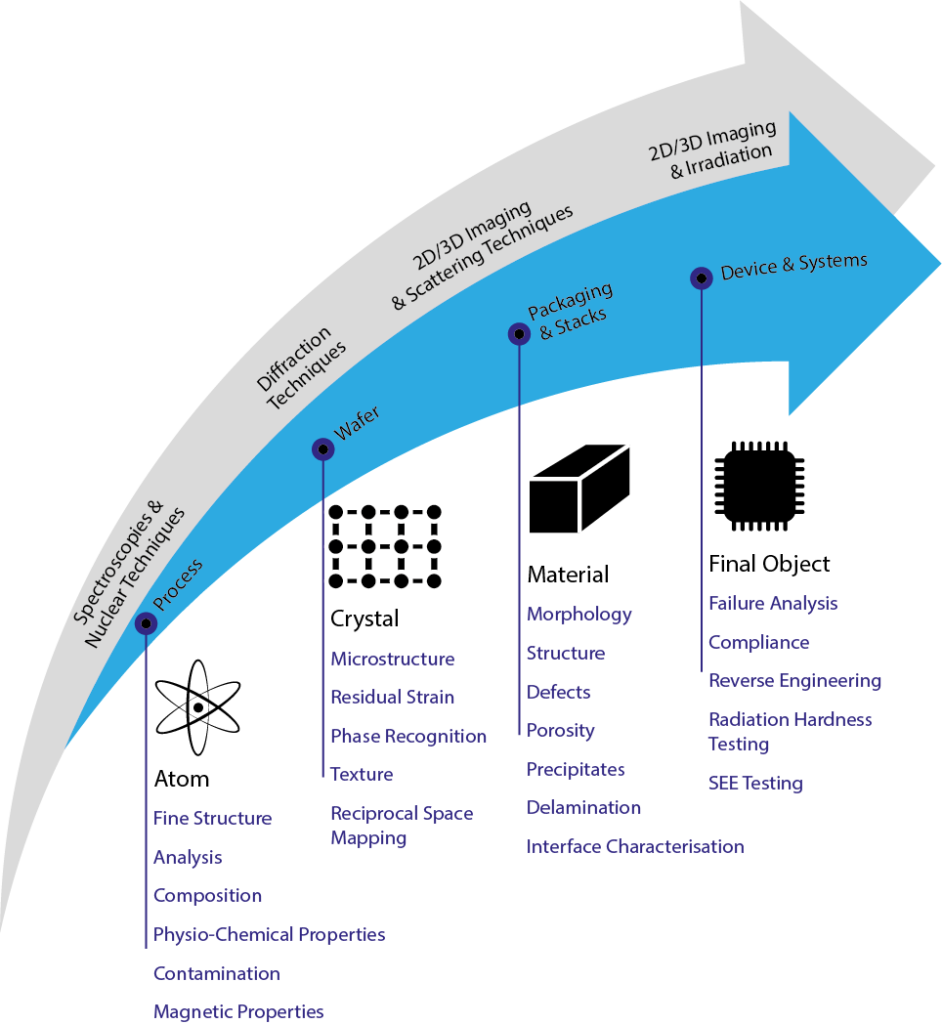
The illustration below shows how the different characterisation techniques offered by PAC-G apply to different length scales and can provide different types of information.
Documentation
The following are technical notes highlighting key application areas that are supported by PAC-G. Each set of notes includes detailed information about an individual characterisation technique. Download links are provided for each file