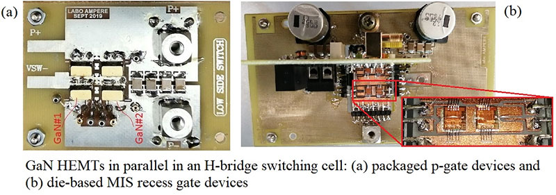
The 22nd European Conference on Power Electronics and Applications held in digital mode in September. Thilini Wickramasinghe (Lyon University) presented a paper on electrical property variability of GaN transistors in parallel and their impact on fast switching operations. Brought by Laboratoire Ampere (Insa Lyon) and CEA-Leti, the study aims to identify the acceptable dispersion range of the electrical properties of transistors in parallel to obtain a stress-free switch operation aiming for medium power (1-3 kW) applications. In this study, both board parasitics and device electrical parameter discrepancies (i.e. threshold voltage in 10% and on-resistance in 25%) were investigated.
“We used 650 V GaN devices with two different gate types (p-gate and MIS-recess gate) in different packagings for the experimental study. It was found that the variation of the threshold voltage can make a high current imbalance during on-transitions while the on-resistance in steady-state has less impact. However, the routing parasitic components in a very high-frequency range have a high influence on current unbalances among the devices compared to the device parameter discrepancy range in the sample. This again proved that the GaN transistor-based designs are appropriate for circuit integrations”, Wickramasinghe says.

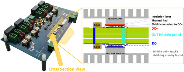
At the EPE’20 also, authors from CNRS, Grenoble-INP (UGA), G2ELab, ENS Cachan and Gdansk University (Poland) made a contribution on the adaptation of a 3D integration concept previously used with vertical devices to lateral GaN devices.
“This 3D integration allows to reduce loop inductance, to ensure more symmetrical design with especially limited Common Mode emission, thanks to a low middle point stray capacitance. This reduction has been achieved by both working on the power layout and including a specific shield between the devices and the heatsink”, underlines Pawel Derkacz, first author of the paper. “Superior performances of the 3D layout are expected when looking at simulation results”, estimates Derkacz.


