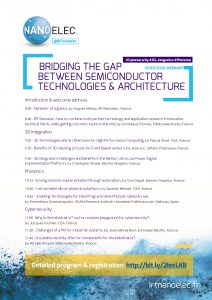
![]() On March 13, 2020, IRT Nanoelec hold a webinar workshop “Bridging the gap between semiconductor technologies and architecture” design focussed on 3D integration, Photonics & Cybersecurity.
On March 13, 2020, IRT Nanoelec hold a webinar workshop “Bridging the gap between semiconductor technologies and architecture” design focussed on 3D integration, Photonics & Cybersecurity.
Additional contents to the workshop 13/3/2020
Video here.
Introduction
IRT Nanoelec at a glance
Hugues Metras, IRT Nanoelec, France
-
- See Hughes slides
- About the talk : The presentation will briefly introduce the workshop, the mission of Nanoelec, its members and activities. A specific highlight will be provided on projects and results that demonstrate how device technologies meet new applications through IC design and novel circuit architectures.
- About the speaker: Hughes Metras has been appointed director of the technological research institute IRT Nanoelec on September 1st, 2019. Previously, he was in charge of strategic partnerships for the US region where he established CEA Leti’s commercial office in 2011. He benefits from a technical background in Physics engineering (Ecole Centrale de Marseille) and holds an MBA from the University of Miami (Florida).
- Related URL
IRT Nanoelec: how to combine multi-partner technology and application research in innovative technical fields, while getting concrete results in the end
Dominique Thomas, STMicroelectronics, France
-
- About the talk: IRT Nanoelec has been used by ST where consortium R&D is most appropriate, that is upstream domains for sharing risks when target application is not well defined. It has associated equipment makers, software vendors, academic labs, and system companies to get feedback from applications. IRT has proven flexible enough to re-target the initial goals for instance from data centric approach to sensor centric for silicon photonics. It has also achieved interesting results in imagers from its 3D integration program, which was initially devoted to memory/logic. ST is looking forward to renew similar successes in the upcoming configuration of the IRT.
- About the speaker: Dr. Thomas has held R&D management positions in the industry, during his 30-year carrier, both in semiconductor and application fields such as Optronics or environmental sensing. From 2009 to 2018, he was the Director of the “Centre Commun de Microelectronique de Crolles” a joint venture between CEA and ST, which had hosted much of the seminal work of FDSOI. He was also part of the teams which defined and defended the Minalogic competitive cluster (2005/2006) and the IRT Nanoelec project (2010/2011) for the Grenoble ecosystem. and he has proposed several of the pilot line projects aiming at establishing the FDSOI ecosystem in Europe. He is now with Europe and France Public Affairs.
- Related URL
 3D Integration
3D Technologies and Architectures for High Performance Computing
Pascal Vivet, CEA, France
- See Pascal’s slides
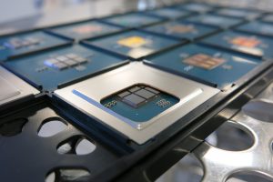
- About the talk: In the context of High Performance Computing (HPC) and scientific computing, the never ending demand of pushing the system performances, targeting power efficient architecture, while reducing the system costs leads to propose disruptive integration schemes. Based on advanced 3D integration, Chiplet-based partitioning offers a cost-efficient heterogeneous integration of a Lego-based optimized HPC system, which is composed of computing chiplets using an advanced technology node, which are 3D stacked on a mature interposer technology node. Pushing the limits further, smart interposer using active circuits allows to add smart features, such as power management, chiplet interconnects, system IOs, and system-on-chip infrastructure. The proposed talk will cover the concept of chiplet-based partitioning, then will present in more details a 96-core architecture prototype composed of 6 chiplets 3D-stacked on a smart interposer, and the corresponding advanced 3D integration technology, including µ-bumps, TSV-middle, and chiplet staking.
- About the speaker: Pascal Vivet is Scientific Director of the Architecture, IC Design and Embedded Software Division in CEA Leti, Grenoble, France. He received his PhD from Grenoble Polytechnical Institute in 2001, designing an asynchronous microprocessor. After 4 years within STMicroelectronics, he joined CEA Leti in 2003 in the digital design lab. His research interests covers wide aspects of circuit and system level design, ranging from system integration, multi-core architecture, Network-on-Chip, energy efficient design, related CAD design aspects, and in strong links with advanced technologies such as 3D integration, Non-Volatile-Memories, photonics. He was project leader on 3D circuit design and integration since 2011. He participates to various TPC such as ASYNC, DATE, 3DIC, ISLPED conferences. He served as a member of the organizing committee of the 3D workshops series at DATE from 2013 to 2015, and to the D43D workshops since 2011. He has authored and co-authored more than 80 papers and holds several patents in the field of digital design. He co-authored a book chapter on “3D Integration in VLSI Circuits: Implementation Technologies and Applications”.
- Related URL
Benefits of 3D stacking process for Event Based sensors
Jean-Luc Jaffard, Prophesee, France
- See Jean-Luc’s slides
- About the talk: 3D stacking processes are very suitable for Image sensor with complex pixel structure composed of many components. During the talk, we will discuss the unique nature of event based sensor and the trade offs to optimize their design using 3D Stacking process. Long-term evolutions of the 3D integration for intelligent image sensor will also be discussed.
- About the speaker: Jean-Luc Jaffard has been graduated from Ecole Supérieure d’Electricité of Paris in 1979. From 1980 to 1996 he occupied various R&D management positions in consumer division of SGS Thomson Microelectronics (initially Thomson Semiconductor) From 1996 Jean-Luc Jaffard paved the way of imaging activity at STMicroelectronics being at the forefront of the emergence and growth of this business. At STMicroelectronics Imaging Division he was successively appointed Research Development and Innovation Director and later on promoted Deputy General Manager. In 2010 he was appointed STMicroelectronics Intellectual Property Business Unit Director. In 2014 he created the Technology and Innovation branch of Red Belt Conseil, bringing expertise in optimisation of complex and innovative solutions to develop competitive products. From 2014 he has been acting as SEMI Europe Imaging conference Chairman. In 2016 he joined Prophesee, French start-up developing biomorphic sensor and processing technology as VP Hardware
- Related URL
3D Integration Challenges and Benefits in the Mentor Ultra Low Power Digital Implementation Platform
Christophe Vinard, Mentor Graphics, France
- About the talk: Mentor, a Siemens business, is providing a complete digital C2GDS implementation platform addressing key market trends such as higher level of abstraction, ultra low power as well as ease of use and automation. HD3D or 3DMonolithic offer new perspectives to create a revolution in the functionality, performance of new electronics systems. This talk will present the current Mentor digital implementation platform along with the challenges and benefits of 3D integration. Mentor and CEA-Leti will partner in the next IRT nanoelec to demonstrate that innovative HD3D technologies are a truly feasible path towards 3DVLSI industrialization for reliable and cost effective products.
- About the speaker: Christophe Vinard has been graduated from Ecole Superieure de Chimie, Physique et Electronique de Lyon in 1998. He received his Master degree of Microelectronics from INSA Lyon the same year. Christophe worked for multiple EDA companies such as Silvaco, Avant!, Synopsys, Sierra Design Automation and Mentor in various position from Application Engineer, Program management, Business development, and Solution Architect. During these 20+ years of experience in semiconductor industry, he acquired a wide knowledge in terms of design implementation platform, in both analog and digital flows.
- Related URL
Photonics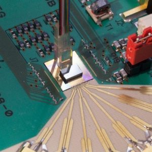
Driving photonic implementation through automation
Tom Daspit, Mentor Graphics, France
- Tom’s slides are available on demand to francois.legrand@cea.fr
- About the talk: Most photonic designs today contain as small number of photonic components. In order for this market to grow, the application space needs to expand and the design ecosystem needs to grow to support this. Today we have multibillion transistor microprocessors that we carry and use every day. This would not be possible without the growth in EDA, and we can use that base of 40 plus years of work to drive photonic design.
- About the speaker: Tom began his career as a full custom design engineer at Gould AMI. Tom has spent the last 25 years working in various EDA applications, sales, and marketing roles. Tom is current a product manager in Mentor ICDS division, responsible for the photonics design tools.
- Related URL
Leti versatile silicon photonics platform
Quentin Wilmart, CEA, France
- See Quentin’s slides
- About the speaker: Quentin Wilmart received the Ph.D. degree in physics from Ecole Normale Supérieure, Paris, France in 2015. He joined CEA-Leti in 2016, working on design, fabrication and characterization of photonic integrated circuits. His current research interests include the use of silicon nitride and IIIV materials for high-speed optical communication and quantum photonics. He is an author or co-author of 23 journal and conference papers and holds several patents.
- About the talk: Silicon photonics enables large volume and low cost production of on-chip photonic components with applications ranging from high-speed optical communication to 3D sensing and quantum computing. CEA-LETI has developed a complete silicon photonics platform, optimizing both design and fabrication processes. We will present our recent progresses including ultra-low loss silicon and silicon nitride waveguides, fast p-n junction modulators, high performance Ge-based photodiodes, and hybrid IIIV-Si integrated lasers.
- Related URL
Enabling Technologies for Field Programmable Photonic Gated Arrays
Prometheus Dasmahapatra , iTEAM Research Institute, Universitat Politècnica de València, Spain
 Cybersecurity
Why is the Industrial IoT such a complex playground for cybersecurity?
Jacques Fournier, CEA, France
- See Jacques’s slides
- About the talk: Industrial IoT, Industry 4.0, smart manufacturing or whichever name one gives to it is one of the most buoyant fields of research and innovation for the Internet of Things. In this presentation, we shall discuss about the major technical security challenges facing an industry which is likely to take the most benefit from the advent of the IoT, especially when looking at the way the devices are being designed, certified, deployed and managed.
- About the speaker: Jacques Fournier is a senior scientist in hardware security at the CEA Leti. He is currently the head of the hardware security lab. Prior to that, he held several technical positions in the Security Lab of smart card manufacturer Gemalto between 2001 and 2009. Jacques obtained his “Habilitation” from the University of Limoges (FR), a PhD from the University of Cambridge (UK), an MSECE from Georgia Tech (USA) and an engineering degree from the French Grande Ecole Supélec.
- Related URL
Challenges of a PKI for industrial systems
Jean-Michel Brun, Schneider Electric, France
- See Jean-Michel’s slides
- About the speaker: Jean-Michel Brun is Chief Security Architect in the IoT and Digital Offer department of Schneider Electric, responsible to support & drive the cyber security of the Digital offers of Schneider Electric as a corporate role. He is also animating the community of Cyber Security Architects of Schneider Electric. Jean-Michel joined Schneider Electric in 1990 and has held multiple positions in R&D, as developer, project manager, software senior architect and cyber security senior architect in OT (Operational Technology), covering embedded device to software, including M2M and industrial cloud. He worked also in Schneider Electric contract department on Automation & Manufacturing Execution System (MES) projects. He managed several French and European innovation projects, targeting cyber security, industrial automation and energy efficiency. He has 4 patents in software and cyber security. Jean-Michel holds a master’s degree in software engineering from CPE Lyon and is ISC² CISSP, ISC² CCSP, GIAC GSEC certified.
- About the talk: Increasingly, PKI (Public Key Infrastructure) is a key part of IT security strategy and customers. Deployment of PKI is a relatively complex operation and request specific competencies to handle this complexity. Within the context of Industrial IoT, smart systems (like smart manufacturing/ Industry 4.0, smart grid etc ) expect OT (Operational technology) components that support certificates to leverage IT grade PKI solutions. In this presentation, we shall discuss about the different technical security challenges an industrial system has to take in implementing a PKI to enable secure communications, data integrity and confidentiality use cases with PKI signed certificates.
- Related URL
A scalable security offer for components for the Industrial IoT
Nicolas Anquet, STMicroelectronics, France
- See Nicolas’ slides
- About the speaker: Nicolas Anquet is principal engineer in hardware architecture for STM32 microcontrollers, at STMicroelectronics (Grenoble).
- About the talk: The fourth industrial revolution, with the Internet of Things (IoT) at its core, is emerging together with a rapidly increasing number of cyber security incidents all over the world. As solution providers, semiconductor technology companies need to help strengthen the cyber resilience of such IoT solutions. This session will explain how the STMicroelectronics portfolio of standard and secure microcontroller components addresses the security challenges related to the evolution of industrial systems and services pushed forward by the introduction of IoT innovations.
- Related URL : STM32Trust, Multi-level strategy to enhance security

