In research conducted under the IRT Nanoelec 3D integration program, a 300 mm hybrid wafer-to-wafer bonding process including ultra-thin (500 nm diameter) copper connections with an optimized pitch of 1μm was successfully demonstrated for the first time worldwide.
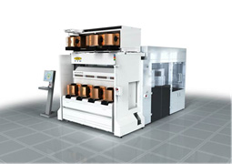
The IRT Nanoelec 3D integration program achieved this major technological advance in Leti’s clean rooms using EVG’s GEMINI®FB XT fully-automated advanced bonding platform.
A finely-honed hybrid copper-oxide bonding process is crucial to the fabrication of high-density 3D integrated circuits. Vertically stacking semiconductor devices has become an increasingly viable approach that will lead to higher density and, ultimately, enhanced peripheral performance. However, wafers must be aligned with extreme precision to ensure good electrical contacts between the devices bonded and to minimize the interconnect zone at the bonded interface, which frees up more functional space on the wafers.
Reducing the interconnect pitch—vital to pursuing the advanced component development roadmap—generates increasingly demanding specifications for the hybrid wafer-to-wafer bonds. The bonds (currently in the hundreds of nanometers) will have to get thinner with each new product generation.
Here, 300 mm wafers were direct-bonded via a hybrid oxide-copper process on the GEMINI®FB XT platform using EVG’s SmartView®NT integrated wafer-to-wafer alignment system and an alignment verification module leveraging in situ infrared measurement. The technique resulted in alignment precision of 195 nm (3 sigma) over the entire bond. After the bonds were annealed, acoustic microscopy and other characterization methods confirmed a defect-free bond interface for pitches from 1 μm to 4 μm with an optimized copper density.
 |
Learn more about our partner EVG’s equipment here: https://www.evgroup.com/en/products/bonding/integrated_bonding/geminifb/?SelectedTab=2


