
Optimiser performance et impact environnemental, le défi des puces 3D
Pour développer des capacités d’écoconception des composants électroniques, le CEA et l’IRT Nanoelec se dotent d’outils d’analyse de cycle de vie (ACV) et d’impact environnemental. Leur tout premier modèle appliqué aux architectures électroniques les plus avancées a été présenté à la conférence IEEE SusTech 2026 (19-22 avril, 2026, California/USA). Leurs premiers calculs démontrent que les stratégies d’empilement des puces peuvent aider à réduire l’impact environnemental des composants si elles aident à développer des composants plus compacts.
En microélectronique, la prise en compte de critères d’impact environnemental, voire sociétal, requiert l’adaptation des procédés de conception et de développement d’un nouveau composant. La communauté scientifique cherche donc à se doter d’outils adaptés, facilitant les analyses de cycle de vie (ACV) afin de systématiser et normaliser des méthodes d’évaluations d’impact dès la phase de conception du composant.
La démarche est très souvent difficile à mettre en œuvre en raison de lacunes ou d’incertitudes dans les ensembles de données indispensables à l’inventaire du cycle de vie. La communauté scientifique manque aussi d’outils performants et normés pour les calculs et les comparaisons.
« Cette difficulté est particulièrement forte pour les composants intégrant des assemblages multipuces, souligne Mathilde Billaud chercheuse CEA, co-autrice d’un article présenté à la conférence IEEE SusTech 2026[1]. Aussi, pour aider à concevoir des assemblages multipuces empilées en 3D, avons-nous conçu et développé un nouveau modèle d’ACV inédit qui ne nécessite qu’un ensemble limité de paramètres de conception. »
Toute première ACV comparative de trois architectures de capteurs d’image
Avec ce modèle de calcul d’ACV, l’équipe du CEA, dans le cadre d’un programme soutenu et financé par l’IRT Nanoelec et le projet européen EECONE, publie la toute première ACV comparative de trois architectures de capteurs d’image CMOS multicouches (CIS)[2]. « Nos résultats montrent que les impacts environnementaux des CIS multicouches sont principalement liés à la fabrication des circuit CMOS. En outre, nous avons constaté que le CIS le plus économe en énergie ne peut compenser ses impacts de fabrication plus importants qu’après une longue période d’utilisation du composant, explique Maxime Peralta, chercheur CEA, premier auteur de la publication. On démontre aussi que l’empilement d’une troisième couche de silicium peut réduire les impacts de fabrication en réduisant la taille de la puce. Ainsi la recherche d’une architecture électronique plus compacte semble une voie vertueuse en termes d’environnement. »
Open source
Le modèle d’ACV proposé et les données environnementales d’intégration 3D sont publiés en open source afin de faciliter de futurs travaux et de contribuer à diffuser largement ces méthodes de prise en compte des impacts au-delà de la figure de mérite PPAC[3]. La publication comprend les résultats ACV de trois briques technologiques nécessaires à l’intégration 3D (amincissement du wafer, collage hybride et TSV haute densité).
« Notre modèle montre que la fabrication de circuits CMOS est généralement la première source d’impact, pénalisant ainsi les grandes puces et l’empilement de couches supplémentaires de circuits, ce qui pénalise également le rendement de fabrication, » poursuit Maxime Peralta. « Néanmoins, l’empilement d’une troisième couche de silicium peut contribuer à réduire la surface totale de silicium et les impacts environnementaux de la fabrication. Les étapes de fabrication supplémentaires requises pour les processus d’intégration 3D entraînent des coûts environnementaux minimes. »
Accélérer l’estimation des impacts environnementaux
Ces conclusions confirment des études précédentes, mais, pour la première fois, elles reposent sur des résultats expérimentaux vérifiables sur plusieurs indicateurs environnementaux. La partie CMOS étant la plus impactante, des études spécifiques d’ACV poussées sont menées en parallèle sur la fabrication de puces CMOS FD-SOI dans le cadre de la ligne pilote FAMES. Elles reposent sur la collecte d’informations précises sur les procédés de réalisation afin d’identifier la contribution de chaque étape de procédé et de comparer des alternatives de fabrication.
Une telle approche de modélisation peut désormais être facilement utilisé pour définir de nouveaux composants car elle ne nécessite qu’un ensemble limité de paramètres de conception. « Ainsi, nous accélérons l’estimation des impacts environnementaux des composants pendant la conception, ouvrant ainsi la porte à des démarches d’éco-conception », souligne Maxime Peralta.
[1] PPAC, pour « Power, Performance, Area & Cost » est une figure de mérite pour l’optimisation de nouveaux composants électroniques, uniquement basée sur des critères technologiques.
[2] IEEE Conference on Technologies for Sustainability (SusTech 2026, 19-22 avril 2026, Californie/USA)
[3] Les calculs sont réalisés pour trois CIS différents décrits dans la littérature.

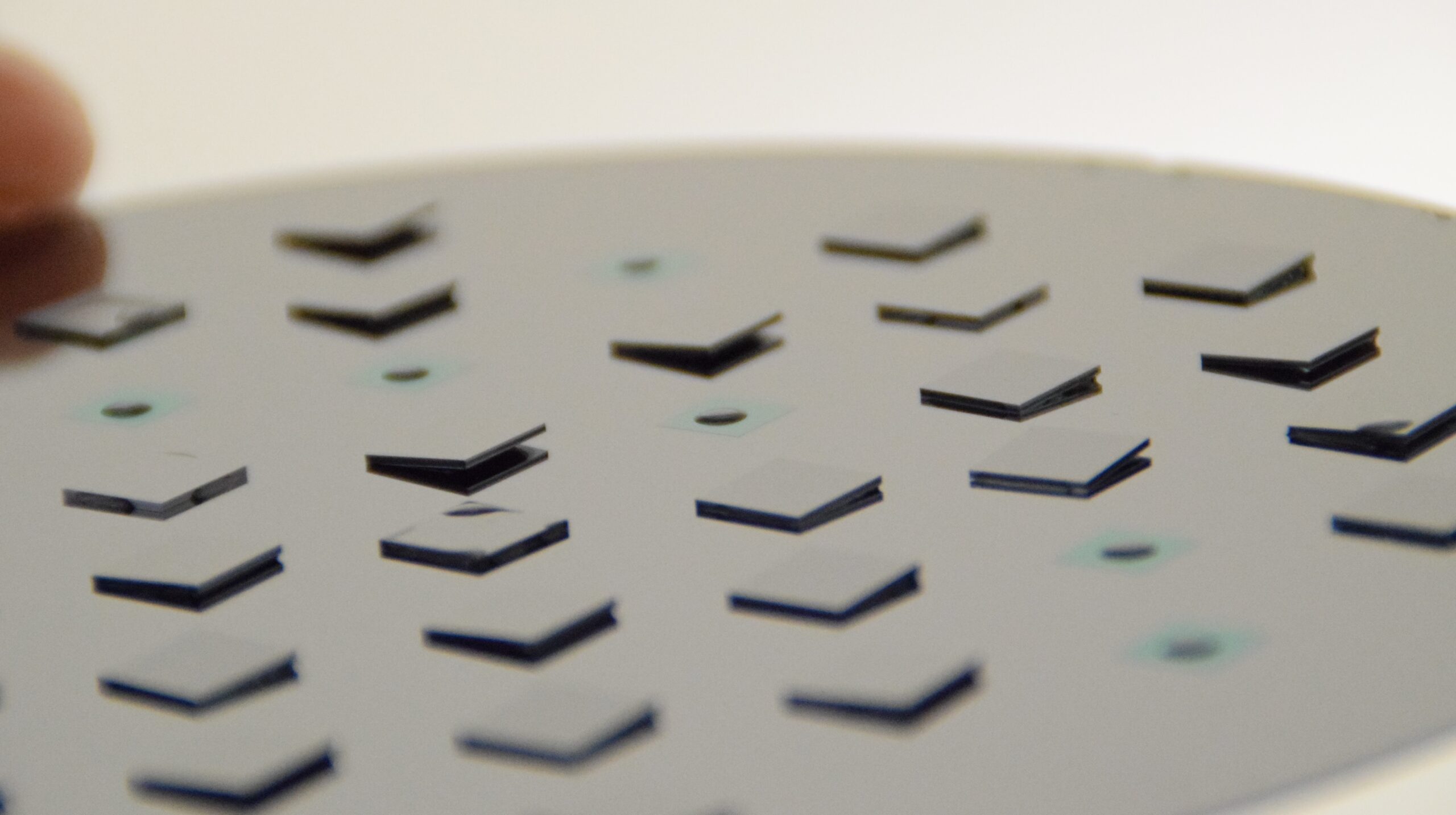
Les stratégies d’empilement des puces pourraient aider à réduire l’impact environnemental des composants si elles aident à développer des composants plus compacts (c) CEA/Barbier