

Over the past five years, 3D integration has gradually become the new standard for low-power image sensors. The idea is to fabricate a CMOS processing circuit and an image sensor in parallel, and then to assemble them as closely as possible.
Using 3D integration, the image sensor can effectively be given its own processing (HDR processing, people recognition, etc.) capabilities.
The concept of 3D integration initially addressed mobile applications. However, the technology now targets a broad range of applications, particularly in the automotive industry, where it has the capacity to accommodate additional features while reducing component form factor and energy consumption.
Of the different 3D integration technologies available, direct hybrid bonding presents several advantages. It is compatible with wafer-to-wafer assembly (which enables higher production throughputs and the ability to continue integration after the wafers are assembled at the foundry) without adding materials (for increased flexibility and optimized thermal management). In addition, the technology enables interconnect pitches of less than 10 µm.
The partners of the IRT Nanoelec 3D integration program developed this technology and used it to design, develop, and test the Harmony demonstrator.
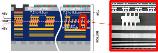
Harmony, illustrated below, was designed with an interconnect pitch of 1.44 µm at the bonding interface. The tiny distance between the interconnections makes sense both in terms of increasing the number of interconnections between the two circuits and aligning the logic circuit as closely as possible with the image sensor’s pixel pitch. The cross section on the right shows an interconnection of around 0. 5 µm².
Once the partners had found solutions to all of the challenges raised by the proposed integration architecture (preparing the surfaces for bonding and precision-assembling the wafers, typically to within 200 nm for 300 mm wafers), the demonstrator chip was cut out and assembled for electrical and optical testing. The robust integration also passed a battery of reliability tests.
Overall, the demonstrator did very well on the tests. This world-first positions IRT Nanoelec and its partners ahead of the current state of the art in 3D integration.
The photograph below was taken with a Harmony sample to show that the image sensor works and that it performs in line with the initial specifications.

This groundbreaking research was the subject of a paper accepted at the prestigious International Electron Devices Meeting (IDEM) held in December 2018 in San Francisco.
The partners are building on their results to pursue even greater levels of performance, with the goal of developing a new generation of smart image sensors that use less energy and deliver added features.