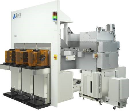
Through an ongoing joint development partnership with Nanoelec, Lam Research, a a leading US supplier of semiconductor processing equipment. has been establishing a suite of enabling process solutions for GaN semiconductor device fabrication. Key to these capabilities is an atomic layer etch (ALE) based process that can provide ultra-low damage, atomic scale precision etching of GaN and related materials. The new, optimized processes can reduce the post etch sheet resistance of the as etched GaN / AlGaN whilst the surface roughness of the etched material remains comparable to that of the incoming epitaxial layers. Such high precision, low damage etch capabilities are critical to the formation of p-GaN or recessed gate HEMT architectures used to fabricate normally off GaN devices for power electronics applications. The development work has been carried out with Lam equipment installed at CEA-Leti and using substrates and analysis capabilities furnished by Nanoelec and CEA-Leti. David Haynes, Managing Director and Head of Specialty Technologies Strategy at Lam, explains.
What are the key applications that the technology being developed by Lam can serve?
Wide band gap semiconductor materials can address a wide variety of applications. GaN particularly has huge potential in high power and high frequency applications. GaN HEMTs are already outperforming Si based super junction MOSFETs in rapid charging applications and GaAs HEMTs in RF devices. In our collaboration with Nanoelec, we have focused on GaN on Si based HEMT and monolithically integrated IC devices for power management applications. However, we are already applying the learning to key GaN on Si RF applications and anticipate in the future that the same process capabilities can bring benefits to the fabrication of other GaN based devices such as micro-LEDs.
Can the atomic layer etch (ALE) process offer a good, commercially viable technique of fabrication of GaN devices?
Atomic layer etching is already widely proven in CMOS based processes where high-precision, highly selective etching is required. Lam has been a pioneer of this technology and our systems are running ALE based applications in high volume manufacturing. Lam began work on ALE of GaN several years ago and found it to be a highly effective process. Indeed, the ideality of the ALE process (the amount of material removed during the ALE step itself vs the surface modification of sputter steps) for GaN is actually superior to that observed for established ALE based processing of Si and dielectrics. But it has taken Lam and Nanoelec working together to fully optimize the process conditions and get the best possible results. Despite the benefits of ALE in terms of uniformity, precision, low damage and selectivity, the rate of removal of the etching material during the ALE process is low compared with conventional etch processing. But the solution is to combine a low damage ALE process with a conventional steady state etch process to offer our customer the benefits of both in a single process sequence
How are the processes combined, and what are the key advantages that have been demonstrated during the project with Nanoelec?
In the process sequences developed with Nanoelec, we first use a fully optimized steady state process to etch the bulk of the AlGaN / GaN structure. This has the advantage of high etch rate and hence short process time, but a steady state process alone, even one that uses very low powers, still results in significant damage to the GaN surface. In turn this leads to sub optimal device performance. So in the processes sequences that we have developed, ALE process steps are added to allow for ultra-low damage etching in the final stages of the process as the etch approaches the highly sensitive 2D electron gas (2DEG) layer that forms the channel of the device at the interface of the AlGaN and GaN. The ALE approach results in a 2X improvement in post etch sheet resistance of the AlGaN / GaN layers and a significant improvement in the electron mobility in the channel compared to even a highly optimized, ultra-low power steady state process alone. We can even build a low damage dielectric mask etch into the process sequence, allowing the full structure to be processed in multiple steps but in a single process module. And Lam’s unique chamber clean and conditioning technologies allow this to be done without “process memory” effects impacting the reproducibility of the approach.
What other challenges are there in the high-volume manufacturing of GaN devices than Lam is working on?
In addition to the etch applications that I have already discussed, there are numerous other plasma deposition and clean process steps that are also critical to improving GaN device performance. Notably, the passivation of the GaN transistor gates is an area where improvements in passivation quality and reduction in plasma induced damage during the deposition processes could have a significant benefit on device performance. So, we are also working to optimize both the passivation process itself and the pre-passivation surface cleaning of the wafers using Lam’s single wafer clean solutions. And while we are talking about single wafer clean, one of the key potential advantages of GaN on Si based technologies is the ability to integrate them into CMOS fabs and foundries. But this creates the need to manage Ga contamination on the wafer backside and bevel and this is another area where Lam is bringing our single wafer clean experience to bare on GaN device fabrications. And of course, there is the overarching challenge associated with transition from 150mm to 200mm wafers. That’s why our approach of developing solutions using established high- volume manufacturing tools makes so much sense; it provides the best 200mm capability while offering a future bridge to 300mm production using the same tools.
What role have Nanoelec played in the development?
All the good work that has been done to demonstrate these capabilities would not have been possible without Nanoelec supplying the test wafers needed to conduct the trials and supporting post process materials characterization and measurement of device electrical properties. Being able to quickly understand the impact on changing process conditions on device outcomes has been fundamental to fully optimizing the processes. During the joint development program, we have been able to establish a library of processes steps that can be built into the necessary processes sequences to address different device architectures.
What have the benefits of working with Nanoelec been and what are the next steps?
One of Lam’s key business philosophies is to deliver “speed to solution” to our customers, and the partnership with Nanoelec has allowed us to achieve this goal. By leveraging the combined subject matter expertise of Lam’s applications engineers and the technical team at Nanoelec, we have been able to deliver solutions ahead of our customers ramping high volume manufacturing of their GaN devices. The solutions developed so far are already being deployed at several leading GaN device players and as we continue to expand our activities with Nanoelec in this area, we expect that our customers will continue to benefit from future, enabling technologies that will result from this highly successful partnership!


