

EV Group, a core partner of Nanoelec consortium, successfully demonstrates end-to-end process flow for collective die-to-wafer bonding with sub-two-micron placement accuracy, (see PR in last october). This breakthrough represents an important milestone in accelerating the deployment of heterogeneous integration in next-generation 2.5D and 3D semiconductor packaging. Such technologies are required for leading-edge applications such as artificial intelligence, autonomous driving, augmented/virtual reality and 5G, all of which require the development of high-bandwidth, high-performance and low-power-consumption devices without increasing production cost. The demonstration was achieved at the EV Group Heterogeneous Integration Competence Center, utilizing existing EVG wafer bonding technology and processes, as well as existing bond interface materials, with substrates provided by Nanoelec and CEA-Leti.

Markus Wimplinger, Corporate Technology Development & IP Director at EV Group (c) EVGroup
Markus Wimplinger, Corporate Technology Development & IP Director at EV Group, explains.
What are for EVG the key benefits (or key applications) of wafer-to-wafer direct hybrid bonding for industry?
In recent years, leading semiconductor companies have stated in public that 3D integration technologies will be part of their next process technology nodes currently under development. This trend has boosted a growth of wafer bonding applications. Wafer bonding was first applied for CMOS image sensor (CIS) manufacturing. Going forward, it is moving to more mainstream applications such as NAND flash memory manufacturing, where hybrid bonding is used at first producers to integrate the cell array with the periphery circuit. Across all fusion and hybrid bonding applications, EVG provides clear technology to hold a dominant market share.
With the increased momentum for 3D integration for future logic devices, wafer bonding may reach some limitations. What are the key gap to enlarge the range of applications using 3D integration?
One key gap for stacking technology is that wafer-to-wafer (W2W) bonding technology is not the only solution required for integrating chiplets with one another. There are many scenarios where die-to-wafer (D2W) integration will be required. Several approaches are under development, more or less mature.
This relates to many of the building blocks involved such as having a clear consensus on the preferred process flows as well as the precision and cleanliness of pick and place equipment. While it would be intuitive to favor direct placement/fusion bonding of the dies in the pick and place equipment directly onto the receiving wafer, there is room for alternatives process flows with collective approach to avoid cleaning and plasma activation of individual dies.
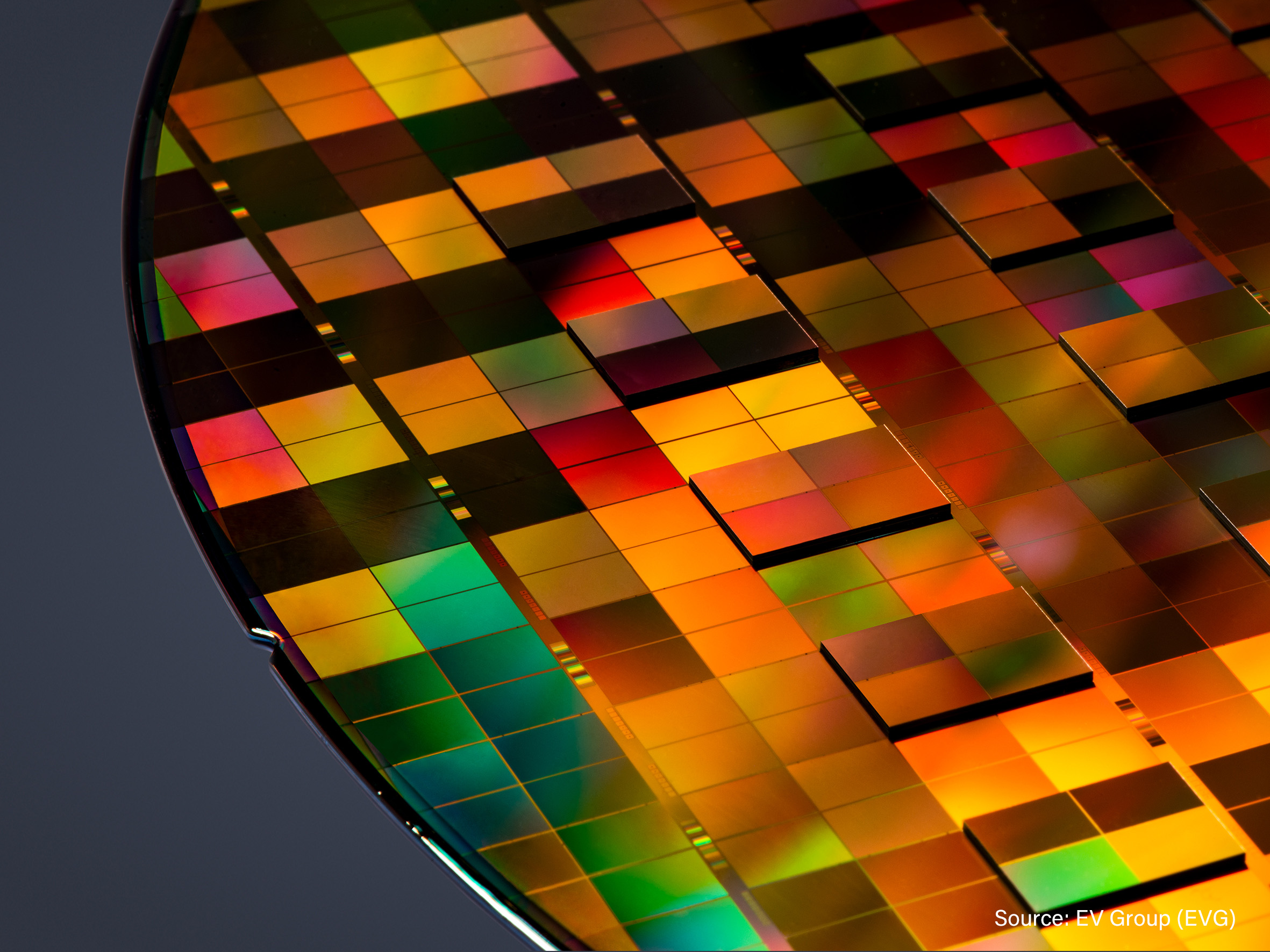
In 2020, EV Group, a core partner of Nanoelec consortium, successfully demonstrates end-to-end process flow for collective die-to-wafer bonding with sub-two-micron placement accuracy © EV Group
How far are you wishing to gain new market or to reinforce your position integrating this new process?
Many people believe that a “collective D2W” bonding flow[1] can be an efficient route toward achieving maturity and high yields for D2W fusion and hybrid bonding. EVG already has installations in the field that support this process flow in high volume manufacturing for non-mainstream semiconductor applications. The work done last year and presented in our press release has resulted in the definition and demonstration of an end-to-end process flow for collective D2W bonding that EVG can now offer to its customers via EVG’s Heterogeneous Integration Competence Center.
Through this work, EVG has improved its industrial standard cleaning and surface activation technology. This could set a new standard for how D2W bonding, and in particular cleaning and surface activation, will be done. Therefore, we expect to reinforce EVG’s leading position with respect to technology and market.
What has been the contribution of Nanoelec to the demonstration of full process?
IRT Nanoelec and CEA-Leti have been providing the wafer material required for this development work. The wafer material was set up to enable hybrid bonding using Cu interconnects. The work would not have been possible without this material. We would like to thank IRT Nanoelec and CEA-Leti for this important contribution.
Will the process be intensively used?
We have clearly seen a huge and growing interest in D2W bonding over the last few years. For this reason, we expect that the process will find significant interest and use in the industry.
What are the benefits for EVG to collaborate in the frame of the French institute Nanoelec?
EVG does not have the capability to prepare adequate test material in-house for such applications. For this reason, the partnership with CEA-Leti in the framework of IRT Nanoelec is very important, as it connects EVG with world-leading capabilities from the other partners in this framework. Moreover, the collaboration allows EVG access to the required materials and technologies and enables EVG to perform leading-edge research and development also.
[1] where the dies are placed on a carrier to be cleaned and plasma activated collectively – through wafer level processing – on this carrier.