

IntAct is IRT Nanoelec’s chiplet on active interposer.
Applications that have particularly high performance requirements—servers and microservers for high-performance computing and hardware accelerators for embedded systems are just two examples—are often built on multicore architectures. These architectures demand increasingly modular circuit designs (to adapt the number of cores). At the same time, circuits are getting bigger (surface area) to the detriment of fabrication yields.
The IRT Nanoelec consortium is banking on 3D integration based on an active silicon interposer to solve these problems. The approach chosen offers all of the advantages of silicon in terms of performance (compared to advanced packaging technologies), but only if it the silicon platform is utilized cleverly. This means embedding active components (currently transistors, and, in the future, optical waveguides) directly on the silicon.
The “active interposer” circuit is partitioned into three dimensions, which makes it possible to divide it into homogeneous chiplets. This enables increased complexity without impacting fabrication yields. The partitioning also allows advanced functions, like circuit-to-circuit communication and power management, to be integrated into the active interposer.
Our IntAct demonstrator chip illustrates the relevance of this type of 3DIC for HPC applications.
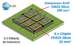
200 mm2 65 nm CMOS active interposer 6 22 mm2 28 nm FDSOI chiplets 2.4 billion transistors
IntAct enables the assembly of a multicore system with 96 32-bit MIPS cores for total power of 96 GOPS. The interposer includes the following differentiating innovations: advanced 3D communications connectors (synchronous and asynchronous providing 800 MHz and 300 MHz of bandwidth, respectively), DC/DC power converters without any external passive components to power each chiplet independently and on demand through the interposer.
This 3D circuit is built on advanced technologies developed at IRT Nanoelec: a large-area active interposer with integrated through silicon vias (TSVs) and a 20 µm interconnect pitch. The interposer’s surface measures 220 mm2 and has 15,000 front-side connections with 15,000 TSVs for estimated power consumption of 10 W. The TSVs are 10 µm in diameter and 100 µm deep. The TSV-Middle vertical, copper-filled connections pass through the silicon and are inserted between the FEOL (the “hot” part of an integrated circuit’s fabrication processes) and BEOL (interconnects) processes. This enables TSVs with a reduced form factor (the height-to-width ratio, generally 10:1), but requires equipment, processes, and—in some cases—materials that are new compared to those conventionally used in CMOS circuit fabrication. The work completed by IRT Nanoelec members benefitted from partnerships related to this program in particular with Aveni, Orbotech, and Applied Materials—most notably for the TSV filling process.
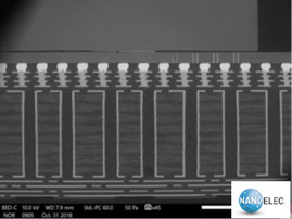
Assembling the circuit was also a challenge, mainly due to the very fine pitch of the interconnects between the chiplets and interposer. The interconnects were made by copper micropillars with a pitch of 20 µm, half the pitch currently used in production. The interconnects were validated by the IRT Nanoelec consortium before they were implemented. Next, the die attach process (chip-to-wafer) and the fill between the chip and wafer were evaluated. Reliability tests completed on IntAct’s embedded testing functions confirmed excellent electrical performance after the chips were attached.
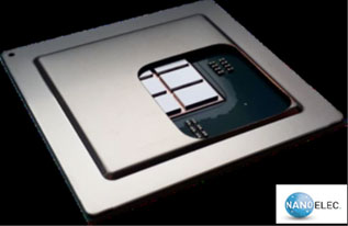
The fully assembled and integrated demonstrator chip was presented at the 2019 IEEE ECTC conference in Las Vegas, a major 3D integration and integrated circuit packaging event.
 |
 |
| Cross-section of the 3D assembly | Rendering of the completed circuit |
IRT Nanoelec presented results that are in line with the state of the art in terms of the requirements of computing applications. In late 2018 Intel unveiled its Foveros technology, and the US Defense Advanced Research Projects Agency (DARPA) initiated its CHIPS program—further confirmation that IRT Nanoelec is on the right track.
Our partners will now push the circuit even further, completing application testing using an application circuit also developed by the program. The partners also plan to submit this research to high-level conferences over the coming year and to transfer the technologies developed to global computing stakeholders.