

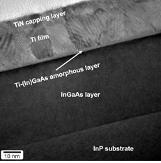
Bright field TEM cross section of the TiN (7 nm) / Ti (20nm)/ InGaAs/InP system in the as-deposited state.
Bensalem et al. recently published in Materials Science in Semiconductor Processing their “Study of the Ti/InGaAs solid-state reactions: Phase formation sequence and diffusion schemes”. The development of Complementary Metal Oxide Semiconductor (CMOS)-compatible contact technology on III–V materials based on Ti for electronics or photonics applications has been studied in the framework of Nanoelec by scientists from CEA-Leti, STMicroelectronics and the Hungarian Academy of Science Center for Energy Research.
“We studied solid-state reactions between Ti thin films (20 nm) and In/Ga/As layers grown on InP substrates from the as-deposited state up to 550°C using a combination of advanced X-ray diffraction (in-plane reciprocal space mapping), Auger electron spectroscopy and transmission electron microscopy analyses” underlines Philippe Rodriguez, as corresponding author for this paper. “The nature of the phases formed above and below the original Ti/InGaAs interface might explain the In accumulation at the interface, the TiAs phase acting as a diffusion barrier. The complete knowledge of the phases in presence and their spatial localization is essential to understand and tailor the electrical properties of the Ti-based contacts on InGaAs. It is also important to anticipate and control the integration scheme impact in terms of additional thermal budget for instance.”