

 Nanoelec has developed groundbreaking research in the area of micro and nanoelectronics since its inception in 2012, resulting in state of the art demonstrators and technology platforms. Mentor, a Siemens business, as the sole EDA (Electronics Design Automation) partner of Nanoelec, is providing design & verification tools for the benefit of the Nanoelec designer community. In addition to providing this valuable support, Mentor also uses the community’s feedback to continually improve its design tools in the context of their performance in use on sophisticated demonstrators and plateforms. Tom Daspit, Product Marketing Manager at Mentor focusses on design & verification tools for Photonics-on-Silicon applications.
Why are design tools essential for enabling growth in photonic design?
Photonics-on-Silicon has a wide range of applications in data center, HPC and telecommunications. The promise of leveraging high-volume, low-cost manufacturing techniques in photonics-on-silicon circuit manufacturing holds the potential to extend the range of photonics applications to smart sensors targeting new spaces such as autonomous vehicles, autonomous robots, healthcare and more.
Extending and leveraging current silicon design tools in order to seamlessly and productively integrate photonics functions with CMOS-based electronics is a key enabler for high volume, high performance photonics circuits.
What are the main methodologies for architecture design in photonics?
Today, there are two main photonic design methodologies: scripted and custom layout. Both are good for creating small designs, but they become inefficient as the design size increases from the 10’s to 100’s to over 1000 components in the design.
Photonic design can benefit from the forty-plus years of industry improvements in IC process technology, methodologies and design tools. Ultimately, the availability of more photonic processes should be able to support much larger designs.
IC design sizes grew from thousands, to millions, to billions of transistors in today’s processors. This growth was enabled by automating IC design tasks. Automation is not just tool-centric, it relies on the underlying design methodology that supports it. An example of digital place and route is LEF/DEF, a standard that abstracts the data to the minimal set that is needed. LEF/DEF is derived from a standard cell design methodology and standard cells are created from individual transistors built up from the data in a Process Design Kit (PDK).
What is the step forward provided by the Mentor LightSuite Photonic Compiler?
Mentor is addressing photonics by supporting both automated and custom layout tools. The EDA leader is focused on driving state of the art layout automation with the Mentor LightSuite Photonic Compiler. The first example below is of a 4 by 4 switch. The layout was automatically created in under 5 minutes.
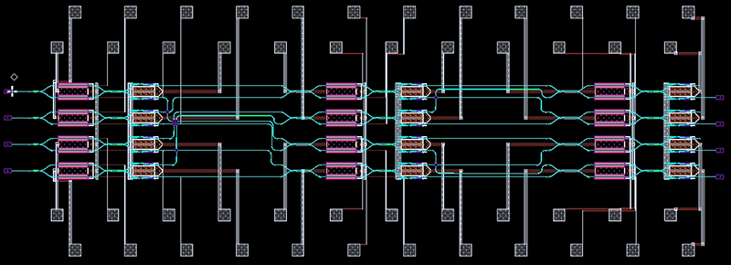
Now scale that switch to a 16 by 16. The complexity of such a change requires complex optical and electrical routing. This DRC clean layout was implemented in 85 minutes. Manual layout of a design of this size would take many months to implement. © Mentor Graphics
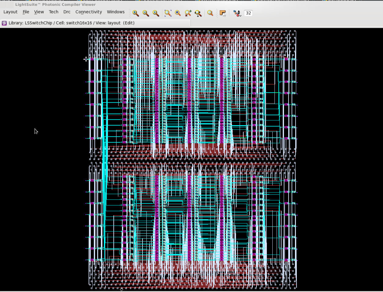
Mentor’s LightSuite Photonic Compiler automatically creates a clean DRC photonic layout, including the corresponding electrical routing. The interface chip that is associated with this switch design has an engineering change order (ECO) — a change is forced in the pin out, which also requires a design change in the corresponding interface chip. That ECO requires about 20% of the electrical pad locations to change. This is not a problem with Mentor’s LightSuite Photonic Compiler, which can generate a new layout in that same 85 minutes. © Mentor Graphics